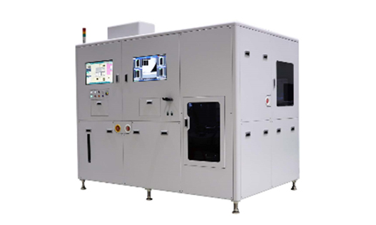
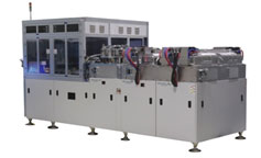
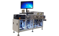
ShieldRus-1200
ShieldRus-1200 is a systemthat performs electromagnetic shielding process
using a sputtering method on semiconductor packages and specializes in mass production.
Key Features
- Compact layout configuration using a cubicle in-line method
- High-speed production capacity
- Easy maintenance
- Ultra low sputtering temp
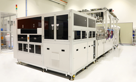
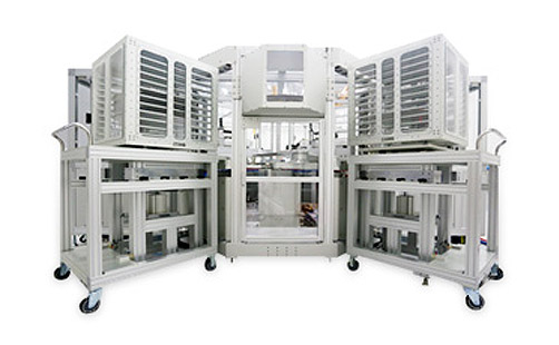
| Item | ShieldRus-1200 | ShieldRus-1200s | ShieldRus-300H |
|---|---|---|---|
| 3D drawing |
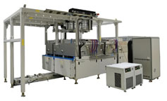
|
|
|
| Tact Time | 6 min(3.5 um at top) | 6 min(3.5 um at top) | 30 min(3.5 um at top) |
| Cooling Type | Active cooling | Active cooling | Active cooling |
| Temperature | < 120℃ (with MF-Seal & Pi tape) | < 120℃ (with MF-Seal & Pi tape) | < 120℃ (with MF-Seal & Pi tape) |
| PKG Handling Material | PI tape and MF-Seal | PI tape and MF-Seal | PI tape and MF-Seal |
| UPH | Ø300 Standard ring frame 40ea | Ø300 Standard ring frame 10ea | Ø300 Standard ring frame 2ea |