Innovative technolgy of EMI shielding
The number of wireless systems embedded in the latest smartphones is increasing in order to improve their functions.
The increase in the speed of clock frequency and data transmission of built-in circuits leads to frequent electromagnetic noises used in wireless systems.
In the past, a “can shield” method at the board level was used to block noise, in which it became an obstacle to downsizing and thinning devices.
To address these issues, a semiconductor package shielding technology was introduced.
The technology reduces the size and thickness of PCB boards by shielding electromagnetic waves at the package level.
In addition, package-shielded semiconductor parts have the advantage of being placeable anywhere on the system boards.
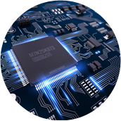
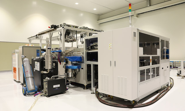
CNI Technology developed an in-line sputtering system that can form high-quality electromagnetic shielding films.
Multiple shielding technology
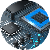
Forming electromagnetic shielding films at the semiconductor package level includes sputtering, plating, and painting.
Because sputtering deposits a shielding film by using a target in a vacuum, it is possible to form a high-density shielding film that is thinner than any other methods.
It also ensures easy thickness control and high yield.
1) VOCs : Volatile Organic Compounds
SIGMA 1000™ technology

-
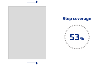
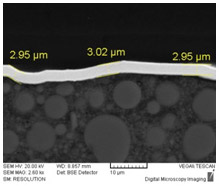
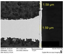
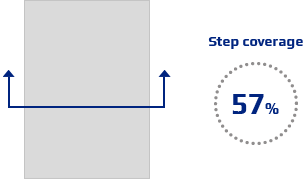
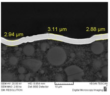
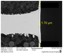
Step coverage
SIGMA1000™ forms a shielding film with more than 50% step coverage by adjusting the tray rotation and sputtering angle.
It maximizes the target use efficiency by depositing a shielding film
with high step coverage, greatly increasing output by shortening the deposition time.

-
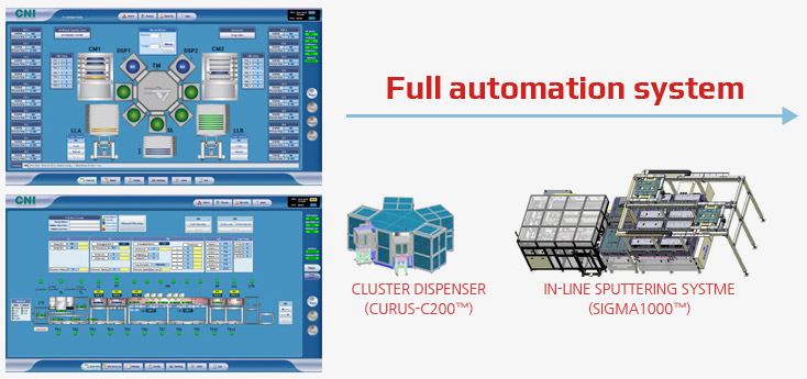
Full automation system
Through an automated system, SIGMA1000™ is optimized for the mass production process.
In particular, we developed materials that are easy to attach and detach (H-VAMs™),
overcoming the limitations of handling semiconductor packages in the conventional taping method.

-
High throughput
SIGMA1000™ maximizes productivity by reducing the gap between semiconductor packages
as much as possible without affecting the step coverage.
We have improved the UPH (unit-per-hour machine rates)
more than twice compared to the existing sputtering equipment by reducing the tact time.

-
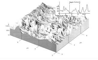
Adhesion property
SIGMA1000™ uses a surface modification treatment through plasma treatment
to improve significantly the adhesion between the molding materials and the shield films of semiconductor packages.
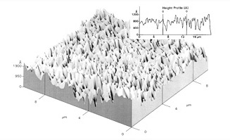
In physical terms, the surface area is increased by improving the roughness of semiconductor packages.
In chemical terms, a change that increases the surface energy occurs
due to an increase in oxygen atoms activated at the interface, a decrease in ion concentration, and a decrease in carbon atoms.
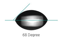
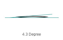
The contact angle measures the change in surface energy.