본문바로가기
Innovative technolgy of EMI shielding

近期,智能手机不断通过增加装载于设备上的无限系统数量提高设备功能。
然而,内置线路的Clock频率与数据传送速度加快后,很容易产生在无线系统中使用的电磁噪音。
过去曾尝试用基板水平的“Can shield”方式屏蔽噪音,但随着设备的小型化和轻薄化发展,这一方法遇到了瓶颈。
为解决这一问题,屏蔽半导体封装本身的全新技术登场。通过在封装水平上屏蔽电磁波,便可实现PCB基板小型化与轻薄化。
另外,进行屏蔽作业的封装半导体元件具有可置于系统基板任意位置的优点。
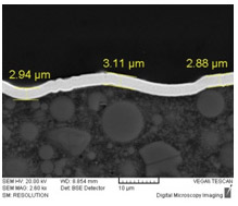
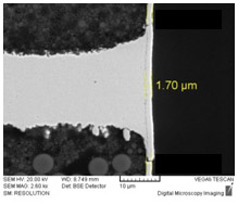
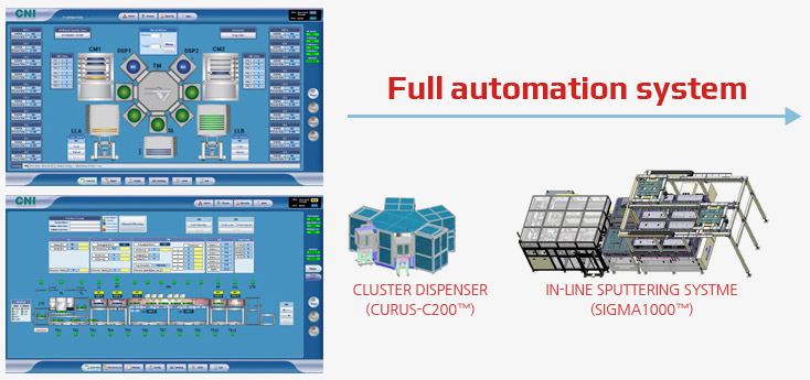
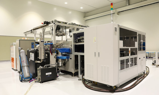
CNI Technology开发出能够形成优质电磁波屏蔽膜的In-line Sputtering系统。

  • Board Level Shielding
    예시이미지

    Shielding i can shield
    (made by stamping and forming a
    piece of conductive metal)

  • Simplified PCB design

    Elimination of external shields from board

    Reduces board area(20 to 30 percent)

    Reduces module height(1.2mm including shield)

    Minimizes rework costs

  • Package Level Shielding
    예시이미지

    Shielding: conformal shield
    (Individual components shield)

Multiple shielding technology

在半导体封装水平上形成电磁波屏蔽膜的方法有溅射、镀金、涂漆等。其中溅射是以真空靶材蒸镀而形成屏蔽膜的方法,
与其他方法相比,可形成高密度屏蔽膜,且具有易于调整厚度、提高良率的优点。

Multiple shielding technology
Sputtering Plating Painting(Spray Coating)
Mvaterials Conductive materials : Cu
Passivation materials : SUS, Ni
Seed layer : Cu
Electrolytic Cu, Ni
Conductive material : Ag, Ag/Cu
Based material : Epoxy, Silicon, Acrylic
Film Thickness ~ 10 um ~ 30 um ~ 100 um
Thickness Control Controllable Variational Variational
Environment VOCs1) Free VOCs Free VOCs
Backside Masking Not necessary Necessary Necessary
Shielding Life Long duration Long duration Short duration
Consumable Materials Target, Process gas Cu, Ni electrolyte Ag, Cu Paint
Yield > 98% N/A N/A
Process Flow
Degassing Plasma
Treatment
Conductive Cu
Sputtering
Passivation SUS
Sputtering
Degassing Plasma
Treatment
Conductive Cu
Sputtering
Passivation SUS
Sputtering
Degassing Plasma
Treatment
Conductive Cu
Sputtering
Passivation SUS
Sputtering

1) VOCs : Volatile Organic Compounds

ShieldRus-1200 technology
아이콘
Step coverage

SIGMA1000™通过旋转托盘与调整溅射角度,可以形成Step coverage达到50%以上的屏蔽膜。
通过溅镀Step -coverage优秀的的屏蔽膜提高靶材的使用效率,缩短蒸镀工艺时间,从而增加产量。

Multiple shielding technology
Section direction Top thickness Side thickness
Step coverage 53% 예시이미지 예시이미지
Step coverage 57% 예시이미지 예시이미지
아이콘
Full automation system

SIGMA1000™为自动化系统,可实现量产工艺最优化。尤其是打破了过去要以胶带方式控制半导体封装的局限,
开发出可以随意装卸的物质(H-VAMs™),从而实现了自动化系统。

제품이미지
아이콘
High throughput

SIGMA1000™在不影响Step coverage的范围内最大限度地缩小半导体封装间距,从而最大程度提高了产量。
另外,还大大缩小了Tact time,与原有溅射设备相比,UPH(unit per hour)得到了超过2倍的提升。

  • 예시이미지
  • 예시이미지
아이콘
Adhesion property

SIGMA1000™通过利用plasma treatment的表面工艺处理,大大提高了半导体封装材料与保护膜之间的Adhesion。
在物理方面,通过改善半导体封装表面的Roughness增加了表面积。
而在化学方面,因为在表面被激活的氧原子增加、离子浓度减少、碳元素减少等效果,出现了表面能量增加的变化。
表面能量的变化,可以用Contact angle测量。

Multiple shielding technology
Before plasma treatment After plasma treatment
AFM Image 예시이미지 예시이미지
Contact angle 68 Degree 4.3 Degree